IBM ships first sub-1nm chip: 0.7nm (7Å) at Albany, ~100B transistors on a nail-sized die
TL;DR
IBM unveils a 0.7nm (7-angstrom) chip — humanity's first sub-1nm node. Density 2× its own 2nm, ~100B transistors on a nail-sized die. Mass production in ~5 years.
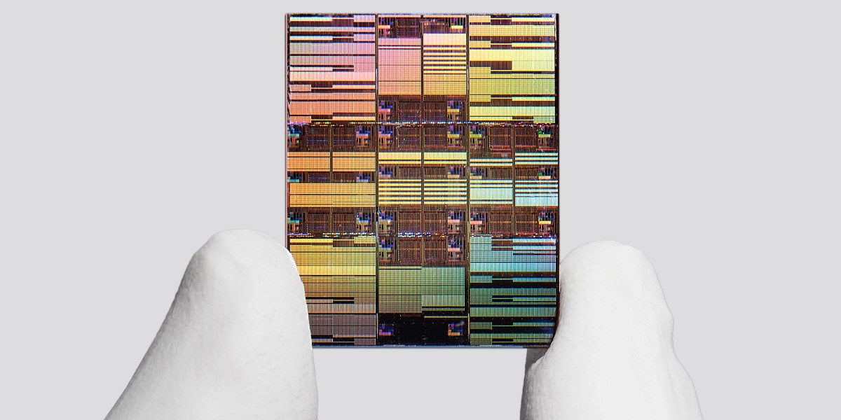
IBM unveiled the world's first sub-1nm chip at its Albany Nanotech Lab on June 25 — node 0.7nm (7 angstroms). The first time mass-production semiconductors formally enter the «angstrom era». Following IBM's 2nm reveal in 2021, semiconductor research has again been led by IBM rather than TSMC or Samsung.
The die is fingernail-sized, integrating ~100 billion transistors — twice the density of IBM's own 2nm process. At iso-power, performance up 50%; at iso-performance, power down 70%; SRAM scaling improves another 40%. For reference, Apple's M4 series sits at ~28 billion transistors per chiplet — 0.7nm puts 3–4× the compute in the same area.
The breakthrough isn't lateral scaling but vertical stacking. IBM calls the architecture Nanostack: 3D sequential stacking of nanosheets, with different layers using different material combinations tuned independently for performance and efficiency. For 40 years, the path has been planar → FinFET → GAA → and now Nanostack: the first generation that fully breaks free of «just shrink lines further».
Partnerships matter. ASML ships the first High-NA EUV machines to Albany. Lam Research, Tokyo Electron, SCREEN join process development. This is the western semiconductor alliance running a complete High-NA EUV demo on US soil — taking the narrative back from Japan's Rapidus and Samsung Korea.
IBM Research lead Jay Gambetta: «This lays the foundation for the next era of computing.» MIT Technology Review's take: Moore's Law can continue at least another decade.
Mass production estimated within 5 years. This isn't a chip consumers can buy this year, but it tells NVIDIA, AMD, and Apple roadmap engineers: the compute ceiling for the next decade isn't the node — it's whether you want to pay for Nanostack.
via IBM Newsroom / MIT Technology Review